Perovskites are a class of materials characterized by a crystal structure that closely resembles that of the mineral calcium titanate (CaTiO₃). This structure has garnered significant attention due to the unique and diverse properties that perovskites exhibit, making them highly valuable in a variety of technological applications. These include photovoltaic (PV) systems, where they are used in solar cells, as well as electronic devices, where their efficiency, stability, and versatility make them ideal for next-generation technologies.
In addition to their practical applications, perovskites are also crucial for exploring quantum states. Researchers are particularly interested in perovskite materials for studying phenomena such as orbital ordering, magnetism, and superconductivity. The ability to fine-tune the properties of perovskites opens new doors for advancing quantum technologies, where small changes in atomic arrangement can lead to dramatically different behaviors. This tunability typically arises from subtle deviations in the ideal cubic perovskite structure, and understanding how to control these deviations is key to unlocking new functionalities.
However, achieving the precise control necessary to induce these small structural changes has historically been challenging. In a recent breakthrough, researchers at the Max Planck Institute for Solid State Research, led by Eva Benckiser, have introduced a new strategy for manipulating the atomic structure of the vanadate perovskite YVO₃. Their study, published in Nature Physics, provides a promising method for controlling subtle atomic displacements in YVO₃, offering new insights into how the functional properties of perovskite materials can be engineered.
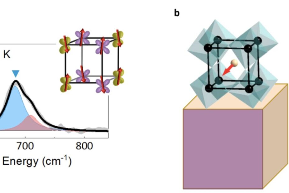
The team’s objective was to understand how the functional properties of a crystalline material like YVO₃ change when it is grown as a thin film on different facets of a substrate. The researchers focused on thin films grown on YAlO₃, a substrate material that has facets with almost identical lattice mismatches with YVO₃. The key innovation of their approach was to grow YVO₃ films in a specific, oriented manner on different facets of the YAlO₃ substrate, while keeping other control parameters, such as lattice and polarity mismatch, nearly the same. This setup allowed the researchers to isolate the effect of slight variations in the atomic displacements at the film-substrate interface, which are often difficult to control in traditional material growth processes.
By using epitaxial deposition methods, where a thin film grows in a controlled orientation on the substrate, the team was able to observe distinct spin-orbital ordering patterns in the vanadate films. These patterns are linked to the interactions between the spins of the electrons and their orbital motion, which is a critical factor in determining the material’s magnetic properties. In materials like YVO₃, which are known to exhibit strong electron-electron correlations, even the smallest structural changes can have significant effects on the material’s properties. The researchers found that depending on which facet of the substrate the film was grown on, the spin-orbital ordering in the YVO₃ films was different.
The results of their study demonstrate that the facet of the substrate can be a powerful tool for controlling the magnetic and electronic properties of perovskite films. This approach allows researchers to imprint atomic displacements in a controlled manner, which could be used to tailor the spin-orbital behavior of materials. The ability to fine-tune these properties opens up new possibilities for designing advanced materials with specific functionalities, such as spintronic devices, where the spin of electrons is used for information processing rather than just their charge.
In their experiments, the team employed light scattering techniques to observe the magnetic ordering patterns in the films. These patterns varied depending on the substrate facet, and the researchers attributed these differences to the subtle atomic displacements induced at the substrate-film interface. This observation suggests that the fundamental effect of imprinting atomic displacements could be used to stabilize desired phases in perovskite materials, potentially leading to the development of novel spintronic or quantum materials.
The findings of this study have significant implications for the precise engineering of quantum materials. By offering a new method for manipulating the structural and magnetic properties of perovskite films, the research provides physicists with an alternative route for creating materials with tailored quantum behaviors. The ability to control spin-orbital interactions in this way could lead to advancements in technologies such as quantum computing, where the manipulation of electron spins plays a key role.
Looking ahead, Benckiser and her team plan to extend their work by investigating the length scale of the orthorhombic displacements imprinted in the films. They also intend to explore the influence of different substrate facets on the properties of other functional perovskite thin films. This ongoing research will help refine the understanding of how small structural changes can affect the behavior of quantum materials, paving the way for the design of next-generation materials with customized properties.
